
2.4GHz Multi-channel FBAR-based TX and PA

Image of chip design
A 2.4GHz TX in 65nm CMOS defines three channels using three high-Q FBARs and supports OOK, BPSK and MSK. The oscillators have -132dBc/Hz phase noise at 1MHz offset, and are multiplexed to an efficient resonant buffer. Optimized for low output power ≈-10dBm, a fully-integrated PA implements 7.5dB dynamic output power range using a dynamic impedance transformation network, and is used for amplitude pulse-shaping. Peak PA efficiency is 44.4% and peak TX efficiency is 33%. The entire TX consumes 440pJ/bit at 1Mb/s.

Multi-channel 180pJ/b 2.4GHz FBAR-based Receiver

Image of chip design
A three-channel 2.4GHz OOK receiver is designed in 65nm CMOS and leverages MEMS to enable multiple sub-channels of operation within a band at a very low energy per received bit. The receive chain features an LNA/mixer architecture that efficiently multiplexes signal pathways without degrading the quality factor of the resonators. The single-balanced mixer and ultra-low power ring oscillator convert the signal to IF, where it is efficiently amplified to enable envelope detection. The receiver consumes a total of 180pJ/b from a 0.7V supply while achieving a BER=10-3 sensitivity of -67dBm at a 1Mb/s data rate.

Voltage Scalable Zero-Crossing Based Pipelined ADC

Image of chip design
A voltage scalable zero-crossing based (ZCB) pipelined ADC is built in 65nm GP process. The highly digital implementation characteristic of the zero-crossing based circuit technique enables energy efficient operation and supply voltage scaling. A unidirectional coarse-fine charge transfer scheme is developed to allow low-voltage operation as well as high resolution. At 1.0V nominal supply and 50MS/s, the ADC achieves 67.7dB SNDR after calibration while dissipating 4.07mW resulting in an FOM of 41.0fJ/step. The supply voltage scalability is demonstrated down to 0.5V and improves the FOM to 28.0fJ/step, while maintaining higher than 66dB SNDR.

A 10pJ/cycle Ultra-Low Voltage 32-bit Microprocessor System-on-Chip

Image of chip design
A voltage-scalable 32 b microprocessor system-on-chip (SoC) that provides both moderate peak performance (up to 82.5MHz at 1.2 V) and extreme energy efficiency (10.2 pJ/cycle at 0.54 V) for applications with limited energy budgets and time varying processing loads is presented. The SoC employs low-voltage 8T SRAMs operating down to an array voltage of 0.4V. Memory access energy is further reduced by miniature (128 B) latch-based instruction and data caches. On chip clock generation and the ability to boot from a small external serial flash ROM makes for a very small overall system.

Quad Full-HD Transform Engine for Dual-Standard Low-Power Video Coding

Image of chip design
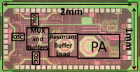
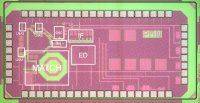
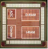
Transform engine is a critical part of the video codec and increased coding efficiency often comes at the cost of increased complexity in the transform module. In this work we propose a shared-reconfigurable transform engine for H.264/AVC and VC-1 video coding standards, using the structural similarity and symmetry of the transforms for H.264/AVC and VC-1. An approach to eliminate the need for an explicit transpose memory in 2D transforms is proposed. Data dependency is exploited to reduce power consumption. Ten different versions of the transform engine, such as with and without hardware sharing, with and without transpose memory, are implemented in the design. The design is fabricated using commercial 45nm CMOS technology and all implemented versions are verified. The shared-reconfigurable transform engine without transpose memory supports Quad Full-HD (3840x2160) video encoding at 30fps, while operating at 0.52V, with measured power of 214 µW.

A Resolution-Reconfigurable 5-to-10b 0.4-to-1V Power Scalable SAR ADC

Image of chip design
A resolution-reconfigurable 5-to-10b SAR ADC for micro-power sensor nodes is implemented in a low-leakage 65nm CMOS process, operating from 2MS/s at 1V to 5kS/s at 0.4V, with power that is linear with sample rate. The DAC power and ADC input capacitance scale exponentially with resolution, and voltage scaling further reduces the energy-per-conversion. Leakage power-gating is applied at low sample rates to reduce the minimum energy point of the ADC. The figure-of-merit is 22.4fJ/conversion-step in 10b mode at 0.55V.