
Application-specific SRAM using Output Prediction and Statistically-Gated Sense Amplifier

Image of chip design
This work proposes an application-specific SRAM design targeted towards video and imaging applications where data stored in the memories is highly correlated. The design utilizes this correlation to reduce bit-line switching activity and uses signal statistics to implement a statistically-gated sense-amplifier approach to achieve up to 1.9× lower energy/access when compared to a standard 8T bit-cell based design. Test chip features 32Kb of the proposed design along with 32Kb of the standard 8T design to provide on-fly comparisons of energy/access between the two implementations.

Scalable 1Mb/s eTextile Body Area Network

Image of chip design
An eTextiles body area network is designed across multiple layers for managing a group of biomedical sensors on a user's body. The sensors are powered remotely by a central base station that also manages data flow in both directions, using modulation schemes chosen to reduce communication effort at the energy-constrained sensors. Power and data are transferred across a magnetic near-field link formed by screen-printed inductors on fabric. Fabricated in 0.18µm CMOS, the base station consumes 2.9 mW power to connect to one sensor node consuming 34µW power and transmitting at 1 Mb/s. This results in an 8× increase in data rate and 6× increase in end-to-end power transfer efficiency than other solutions.

Application-specific SRAM using Output Prediction and Statistically-Gated Sense Amplifier

Image of chip design
This work proposes an application-specific SRAM design targeted towards video and imaging applications where data stored in the memories is highly correlated. The design utilizes this correlation to reduce bit-line switching activity and uses signal statistics to implement a statistically-gated sense-amplifier approach to achieve up to 1.9× lower energy/access when compared to a standard 8T bit-cell based design. Test chip features 32Kb of the proposed design along with 32Kb of the standard 8T design to provide on-fly comparisons of energy/access between the two implementations.

18.5kHz RC Oscillator with Comparator Offset Cancellation

Image of chip design
A fully-integrated 18.5kHz RC time-constant-based oscillator is designed in 65nm CMOS for sleep-mode timers in wireless sensors. A comparator offset cancellation scheme achieves 7x temperature stability improvement, leading to an accuracy of ±0.25% over -40 to 90°C and ±0.1% over 0 to 90°C. Sub-threshold operation and low-swing oscillations result in ultra-low power consumption of 120nW. The oscillator has a long-term Allan stability of 20ppm or better for measurement intervals over 0.5s.

EEG Acquisition SoC with Siezure Classification

Image of chip design
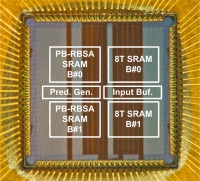
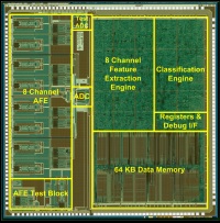
An 8-channel scalable EEG acquisition SoC is presented to continuously detect and record patient-specific seizure onset activities from scalp EEG. The SoC integrates 8 high-dynamic range Analog Front-End (AFE) channels, a machine-learning seizure classification processor and a 64KB SRAM. The classification processor exploits the Distributed Quad-LUT filter architecture to minimize the area while also minimizing the overhead in power×delay. The AFE employs a Chopper-Stabilized Capacitive Coupled Instrumentation Amplifier to show NEF of 5.1 and noise RTI of 0.91µVrms for 0.5-100Hz bandwidth. The classification processor adopts a support-vector machine as a classifier, with a GBW controller that gives real-time gain and bandwidth feedback to AFE to maintain accuracy. The SoC is verified with the Children's Hospital Boston-MIT EEG database as well as with rapid eye blink pattern detection test. The SoC is implemented in 0.18µm 1P6M CMOS process occupying 25 sq.mm, and it shows an accuracy of 84.4% in eye blink classification test, at 2.03µJ/classification energy efficiency. The 64 KB on chip memory can store up to 120 seconds of raw EEG data.

Mixed-signal ECG Front-end

Image of chip design
A mixed-signal ECG front-end that uses aggressive voltage scaling to maximize power-efficiency and facilitate integration with low-voltage DSPs is implemented in a 0.18µm CMOS process. 50/60Hz interference is canceled using mixed-signal feedback, enabling ultra-low-voltage operation by reducing dynamic range requirements. Analog circuits are optimized for ultra-low-voltage, and a SAR ADC with a dual-DAC architecture eliminates the need for a power-hungry ADC buffer. Oversampling and ΔΣ-modulation leveraging near-VT digital processing are used to achieve ultra-low-power operation without sacrificing noise performance and dynamic range. The fully-integrated front-end consumes 2.9µW from a 0.6V supply.