
A Resonant Receiver with Maximum Efficiency-Tracking for Device-to-Device Wireless Charging

Image of design
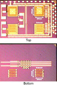
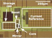
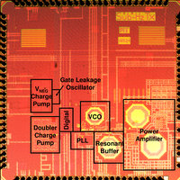
The growing number of IoT devices calls for new solutions for efficient power delivery that are also more scalable than wired systems. Energy harvesting in an indoor environment is usually limited in output power, while wireless charging using near-field magnetic coupling requires close proximity between the Tx and Rx. In order to recharge these devices without affecting their operation, this work proposes using portable transmitters by adding wireless charging capability to smartphones, for example. In such a system, maximizing system efficiency throughout the entire charging cycle instead of output power becomes the primary concern. The receiver IC consists of a resonant rectifier implemented using synchronously driven, on-chip switches and off-chip passives that reduces switching losses and lowers switch voltage stress. The system also implements a maximum system efficiency-tracking loop that requires no explicit communication with the Tx. The receiver IC includes analog sense circuitry for the tracking loop and a boost regulator at the output of the rectifier. The analog measurements are digitized by an off-chip microcontroller, which calculates the efficiency and moves the operating point of the system towards the maximum efficiency-point by changing the duty cycle input of the boost regulator.

A Vertical Solenoid Inductor for Noise Coupling Minimization in 3D-IC

Image of chip design
This chip presents the use of an integrated solenoid inductor in three dimensional integrated circuits (3D-IC) for improved noise mitigation. The structure is fabricated in a two-tier, stacked 28nm CMOS using through silicon vias (TSV). The structure is implemented as part of an LC voltage-controlled oscillator (VCO), and exhibits 6dB improvement in phase noise and 14dB less coupling from adjacent digital clock lines compared to a planar two-turn inductor.

Ultra-low Energy Relaxation Oscillator with 230 fJ/cycle Efficiency

Image of chip design
An ultra low energy oscillator circuit is presented for use in picowatt level systems. The core oscillator uses an 18-transistor 3-stage architecture designed to minimize short circuit current. In addition, a transistor threshold is used to set the trip point as opposed to a voltage reference and comparator scheme, leading to overall energy savings. While operating across a wide range of low frequencies from 18 Hz to 1000 Hz, the oscillator core consumes 110 fJ/cycle at 0.6 V. The circuit is demonstrated alongside an integrated current source to set the reference frequency. The combined system consumes a total power of 4.2 pW at 18 Hz, resulting in 230 fJ/cycle at 0.6 V.

Solar Energy Harvesting System with Integrated Battery Management and Startup Using Single Inductor and 3.2nW Quiescent Power

Image of chip design
A solar energy harvesting chip with 3.2nW quiescent power. The chip integrates self-startup, battery management, supplies 1V regulated rail with single inductor and supports power range of 10nW to 1μW. The control circuit is designed in an asynchronous fashion that scales the effective switching frequency of the converter with the level of the power transferred. The on-time of the converter switches adapts dynamically to the input and output voltages for peak-current control and zero-current switching. For input power of 500nW, the proposed system achieves an efficiency of 82%, including the control circuit overhead, while charging a battery at 3V from 0.5V input. In buck mode, it achieves a peak efficiency of 87% and maintains efficiency greater than 80% for output power of 50nW-1μW with input voltage of 3V and output voltage of 1V.

A +10dBm 2.4GHz Transmitter with sub-400pW Leakage and 43.7% System Efficiency

Image of chip design
A 2.4GHz TX in 65nm CMOS is optimized for extremely low duty-cycle regimes. Negative gate biasing of the main PA transistor in sleep mode achieves a 30x reduction in sleep-mode power without requiring an additional sleep device. The PA achieves a peak output power of +10.9dBm and a total TX efficiency of 43.7%. The TX integrates a PLL and digital baseband for Bluetooth LE operation. Extensive power gating of all blocks results in a total leakage of 370pW for an on/off power ratio of 7.4x10e7.