
A 25 mV-Startup Cold Start System with On-Chip Magnetics for Thermal Energy Harvesting

Image of chip design
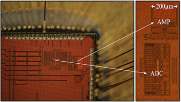
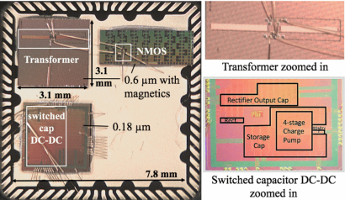
Thermal energy harvesting systems use boost converters for high-efficiency low voltage operation, but lack the ability for low voltage startup without off-chip transformers. We present a cold start system that uses integrated magnetics instead of external transformers in a Meissner Oscillator to start up from ultra low voltages, with a switched capacitor DC-DC circuit for additional voltage gain. The oscillator analysis with on-chip magnetics allows device co-optimization for low voltage operation, despite 1000x lower inductance values than off-chip transformers. Co-optimized on-chip transformer and depletion-mode NMOS start up from 25 mV driven directly by a sourcemeter, or 50 mV with a 4.7 Ω series resistance, for the lowest integrated electrical startup. The co-packaged system provides proof of concept for integration with boost converter circuits on a single die to have a fully-integrated low voltage startup solution for thermal energy harvesting applications, without using off-chip transformers.

0.3 V Ultra-Low Power Sensor Interface for EMG

Image of chip design
A low-voltage, ultra-low power sensor interface for electromyogram (EMG) signal acquisition is presented. The sensor interface consists of an amplifier and a SAR ADC that work from a 0.3V supply. The low-voltage amplifier topology provides a noise level of 26μVrms, 40dB gain and a state-of the art power efficiency factor (PEF) of 2.2 from a 20-425Hz bandwidth. Low-voltage supply improves the power efficiency of the amplifier compared with previous ultra-low power work. Together with the ADC, the prototype implemented in 65nm CMOS process consumes 3.8nW and has an area of 0.22mm2, which makes the sensor interface suitable for wearable IoT nodes as well as implantable devices.

Single-BAW Multi-Channel Transmitter with Low Power and Fast Start-Up Time

Image of chip design
This work presents a multi-channel transmitter (TX) architecture that uses only a single bulk acoustic wave (BAW) resonator while covering 88 MHz of bandwidth. The proposed architecture overcomes the limited tuning range of a single BAW resonator by combining the BAW tuning range with a programmable integer-N frequency division and RF single-sideband (SSB) mixing approach. The single-BAW multi-channel TX achieves 88 MHz-wide frequency coverage with 1 MHz channels. It operates in the 2.4 GHz ISM band and the full system is demonstrated with 0 dBm output power and a fast system startup time of 2.3 μs enabled by the BAW resonator. It is implemented in 65 nm CMOS technology in a 2 mm × 2 mm area and consumes 6.4 mW from a 1.1 V supply.

A Fully-Integrated Energy-Efficient H.265/HEVC Decoder with eDRAM for Wearable Devices

Image of Chip design
Data movement to and from off-chip memory dominates energy consumption in most video decoders, with DRAM accesses consuming 2.8x-6x more energy than the processing itself. We present a H.265/HEVC video decoder with embedded DRAM (eDRAM) as main memory. We propose the following techniques to optimize data movement and reduce the power consumption of eDRAM: 1) lossless compression is used to store reference frames in 2x fewer eDRAM banks, reducing refresh power by 33%; 2) eDRAM banks are powered up on-demand to further reduce refresh power by 33%; 3) syntax elements are distributed to four decoder cores in a partially compressed form to reduce decoupling buffer power by 4x. These approaches reduce eDRAM power by 2x in a fully-integrated H.265/HEVC decoder with the lowest reported system power. The decoder chip requires no external components and consumes 24.9-30.6mW for 1920×1080 video at 24-50 fps.