
Ultra-Fast Bit-Level Frequency-Hopping Transmitter for Securing Low-Power Wireless Devices

Image of chip design
Current BLE transmitters are susceptible to selective jamming due to long dwell times in a channel. To mitigate these attacks, we propose physical-layer security through an ultra-fast bit-level frequency-hopping (FH) scheme by exploiting the frequency agility of bulk acoustic wave resonators (BAW). Here we demonstrate the first integrated bit-level FH transmitter (TX) that hops at 1μs period and uses data-driven random dynamic channel selection to enable secure wireless communications with additional data encryption. This system consists of a time-interleaved BAW-based TX implemented in 65nm CMOS technology with 80MHz coverage in the 2.4GHz ISM band and a measured power consumption of 10.9mW from 1.1V supply.

A Low-Power Integrated Power Converter for an Electromagnetic Vibration Energy Harvester

Image of chip design
This work demonstrates the first fully-functional integrated power converter designed to interface a MEMS-based electromagnetic (EM) vibration energy harvester for near-50 Hz operation. The IC accomplishes (i) cold startup from a 50 Hz-150-mV-peak AC input to a 1.1-V output, (ii) conjugate impedance matching for maximum power extraction along with resonant frequency tuning and (iii) input-AC-to-output-DC voltage conversion. Cold startup is achieved using an on-chip Meissner oscillator with an off-chip transformer. Thereafter, a self-timed current-feedback-based H-bridge circuit is turned on for conjugate impedance matching with on-chip control and an off-chip microcontroller for impedance synthesis. The regular-operation H-bridge circuit delivers 820 uW to a load capacitor at 71% efficiency at resonance. It also performs frequency tuning to deliver 650 uW (57%-efficiency) at 50% off-resonance, thereby demonstrating robustness to possible harvester-resonance variations due to manufacturing tolerances. This makes it the first demonstration of a full-system low-power interface IC for vibrational energy harvesters. The prototype is fabricated in 0.18 um CMOS process with an active area of 1.5 mm2.

A −80dBm BLE-Compliant, FSK Wake-Up Receiver with System and Within-Bit Duty-Cycling for Scalable Power and Latency

Image of chip design
This work presents an FSK wake-up receiver with a -80 dBm sensitivity using a packet structure and a duty cycling scheme compliant with the Bluetooth Low Energy (BLE) protocol trading off power with latency. Event-driven applications achieve power lower than 240nW from a 0.75V supply while latency-critical systems wake up in almost 200μW at a 230μW consumption. A within-bit LC oscillator duty-cycling scheme is proposed to provide an extra 24% power reduction. Additionally, a custom FSK transmitter can trigger wake-up at 17nW only for an average latency of 5 seconds.

Conv-RAM: An Energy-Efficient SRAM with Embedded Convolution Computation for Low-Power CNN-Based Machine Learning Applications

Image of chip design
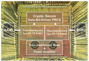
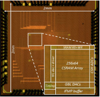
Convolutional neural networks (CNN) provide state-of-the-art results in a wide variety of machine learning (ML) applications, ranging from image classification to speech recognition. However, they are very computationally intensive and require huge amounts of storage. Recent work strived towards reducing the size of the CNNs proposes a binary-weight-network (BWN), where the filter weights are ±1 (with a common scaling factor per filter: α). This leads to a significant reduction in the amount of storage required for the weights, making it possible to store them entirely on-chip. However, in a conventional all-digital implementation, reading the weights and the partial sums from the embedded SRAMs require a lot of data movement per computation, which is energy-hungry. To reduce data-movement, and associated energy, we present an SRAM-embedded convolution architecture, which does not require reading the weights explicitly from the memory. Prior work on embedded ML classifiers have focused on 1b outputs or a small number of output classes, both of which are not sufficient for CNNs. This work uses 7b inputs/outputs, which is sufficient to maintain good accuracy for most of the popular CNNs. The convolution operation is implemented as voltage averaging, since the weights are binary, while the averaging factor (1/N) implements the weight-coefficient α (with a new scaling factor, M, implemented off-chip).

An Energy-Efficient Reconfigurable DTLS Cryptographic Engine for End-to-End Security in IoT Applications

Image of chip design
End-to-end security protocols, like Datagram Transport Layer Security (DTLS), enable the establishment of mutually authenticated confidential channels between edge nodes and the cloud, even in the presence of untrusted and potentially malicious network infrastructure. While this makes DTLS an ideal solution for IoT, the associated computational cost makes software-only implementations prohibitively expensive for resource-constrained embedded devices. We address this challenge through three key contributions: reconfigurable cryptographic accelerators enable two orders of magnitude energy savings, a dedicated DTLS engine offloads control flow to hardware reducing program code and memory usage by ~10x, and an on-chip RISC-V core exercises the flexibility of the cryptographic accelerators to demonstrate security applications beyond DTLS.