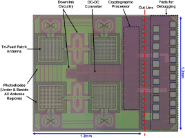
Energy-autonomous wireless tags have been adopted in authentication and supply-chain management. At present, their size and cost, limited by packaging, prevent the tagging for small or inexpensive industrial/medical components. At the same time, pervasive electronic tagging raises serious privacy concerns related to inadvertent and malicious tracking of the tagged assets. In order to enable secure and ubiquitous asset tagging, fully passive particle-sized cryptographic chips without external packaging are highly desired. Recent prototypes that aim to address this challenge face either size, energy, communication, or security limitations. In this work, we present a package-less, monolithic tag chip with built-in photovoltaic powering and a compact elliptic-curve-cryptography (ECC) processor. Using far-field backscatter communication at 260GHz, the CMOS tag, while integrating a 2×2 antenna array with beam-steering capability, has a size of only 1.6mm2.