
Batteryless, Wireless, and Secure SoC for Implantable Strain Sensing

Image of chip design

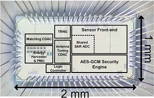
The past few years have witnessed a growing interest in wireless and batteryless implants, due to their potential in long-term biomedical monitoring of in-body conditions such as internal organ movements, bladder pressure, and gastrointestinal health. Early proposals for batteryless implants relied on inductive near-field coupling and ultrasound harvesting, which require direct contact between the external power source and the human body. To overcome this near-field challenge, recent research has investigated the use of RF backscatter in wireless micro-implants because of its ability to communicate with wireless receivers that are placed at a distance outside the body (∼0.5 m), allowing a more seamless user experience. Unfortunately, existing far-field backscatter designs remain limited in their functionality: they cannot perform biometric sensing or secure data transmission; they also suffer from degraded harvesting efficiency and backscatter range due to the impact of variations in the surrounding tissues. In this paper, we present the design of a batteryless, wireless and secure system-on-chip (SoC) implant for in-body strain sensing. The SoC relies on four features: 1) employing a reconfigurable in-body rectenna which can operate across tissues adapting its backscatter bandwidth and center frequency; 2) designing an energy efficient 1.37 mmHg strain sensing front-end with an efficiency of 5.9 mmHg·nJ/conversion; 3) incorporating an AES-GCM security engine to ensure the authenticity and confidentiality of sensed data while sharing the ADC with the sensor interface for an area efficient random number generation; 4) implementing an over-the-air closed-loop wireless programming scheme to reprogram the RF front-end to adapt for surrounding tissues and the sensor front-end to achieve faster settling times below 2 s.

A ThreshoId-ImpIementation-Based Neural-Network Accelerator Securing Model Parameters and Inputs Against Power Side-Channel Attacks

Image of chip design

With the recent advancements in machine learning (ML) theory, a lot of energy-efficient neural network (NN) accelerators have been developed. However, their associated side- channel security vulnerabilities pose a major concern. There have been several proof-of-concept attacks demonstrating the extraction of their model parameters and input data. This work introduces a threshold implementation (TI) masking-based NN accelerator that secures model parameters and inputs against power and electromagnetic (EM) side-channel attacks. The 0.159 mm2 demonstration in 28 nm runs at 125 MHz at 0.95 V and limits the area and energy overhead to 64% and 5.5×, respectively, while demonstrating security even greater than 2M traces. The accelerator also secures model parameters through encryption and the inputs against horizontal power analysis (HPA) attacks.

Randomized Switching SAR (RS-SAR) ADC Protections for Power and Electromagnetic Side Channel Security

Image of Chip design
Analog to digital converters (ADCs) are necessary in most Internet of Things (loT) devices, to link the physical analog world to digital computation. Physical side channel attacks (SCAs) have been used to reconstruct information processed within digital integrated circuits in a variety of applications, through power or electromagnetic (EM) traces [1]. Furthermore, power SCAs have successfully decoded the analog information converted within Successive Approximation Register (SAR) ADCs [2], [3]. Previous works have proposed initial protections, such as switched-capacitor current equalization for power SCAs [2], random dithering for the reference charge [3], or general power side channel security using a stacked digital low dropout array and random noise injection [4]. Whereas power SCAs require cutting the power trace and introducing a shunt resistor for measurement, EM SCAs can effectively perform non-invasive measurements external to packaging (Fig. 1). However, supply current equalization is not effective against localized EM SCAs, which can probe currents directly above the ADC circuitry.

A Bit-level Sparsity-aware SAR ADC with Direct Hybrid Encoding for Signed Expressions for AIoT Applications

Image of chip design
In this work, we propose the first bit-level sparsity-aware SAR ADC with direct hybrid encoding for signed expressions (HESE) for AIoT applications. ADCs are typically a bottleneck in reducing the energy consumption of analog neural networks (ANNs). For a pre-trained Convolutional Neural Network (CNN) inference, a HESE SAR for an ANN can reduce the number of non-zero signed digit terms to be output, and thus enables a reduction in energy along with the term quantization (TQ). The proposed SAR ADC directly produces the HESE signed-digit representation (SDR) using two thresholds per cycle for 2-bit look-ahead (LA). A prototype in 65nm shows that the HESE SAR provides sparsity encoding with a Walden FoM of 15.2fJ/conv.-step at 45MS/s. The core area is 0.072mm2.

RaM-SAR: A Low Energy and Area Overhead, 11.3 fJ/conv.-step 12b 25MS/s Secure Random-Mapping SAR ADC with Power and EM Side-channel Attack Resilience

Image of chip design
This paper presents RaM-SAR, a 12b 25MS/s 11.3fJ/conv.-step secure random-mapping SAR ADC with power and EM side-channel attack resilience. Each conversion is randomly mapped to one of the thousands of conversion sequences to randomize power supply traces. This technique protects against neural network based power and EM side-channel attacks. It enables protection with much lower energy and area overheads compared to the prior works. A prototype in 65nm CMOS demonstrates significant improvements with 12.5× higher bandwidth and 4.8× better energy-efficiency over prior works.

A Dual-Antenna, 263-GHz Energy Harvester in CMOS for Ultra-Miniaturized Platforms with 13.6% RF-to-DC Conversion Efficiency at −8 dBm Input Power

Image of chip design
This paper reports a CMOS energy harvester, which operates at so far the highest reported frequency (263 GHz) in order to realize wireless powering of ultra-miniaturized platforms. To maximize the THz-to-DC conversion efficiency, n, at low available radiation power, the harvester not only utilizes a high-speed 22-nm FinFET transistor but also achieves the optimal operating conditions of the device. In specific, the circuit enables self-gate biasing; and through a dual-antenna topology, it drives the transistor drain and gate terminals with both optimal voltage phase difference and power ratio simultaneously and precisely. With a low input power of −8 dBm, the harvester achieves 13.6% measured conversion efficiency and delivers 22 µW to a 1-kΩ load. Without relying on any external component, the harvester chip occupies an area of 0.61 * 0.93 mm2.

A Threshold Implementation-Based Neural Network Accelerator With Power and Electromagnetic Side-Channel Countermeasures

Image of Chip design
With the recent advancements in machine learning (ML) theory, a lot of energy-efficient neural network (NN) accelerators have been developed. However, their associated side-channel security vulnerabilities pose a major concern. There have been several proof-of-concept attacks demonstrating the extraction of their model parameters and input data. This work introduces a threshold implementation (TI) masking-based NN accelerator that secures model parameters and inputs against power and electromagnetic (EM) side-channel attacks. The 0.159 mm 2 demonstration in 28 nm runs at 125 MHz at 0.95 V and limits the area and energy overhead to 64% and 5.5 × , respectively, while demonstrating security even greater than 2M traces. The accelerator also secures model parameters through encryption and the inputs against horizontal power analysis (HPA) attacks.