
A 50Mb/s UWB Prototype Transceiver

Image of chip design
This prototype transceiver is built using discrete components. It communicates in a 500MHz band centered at 5.355GHz using BPSK pulses with a pulse repetition frequency of 50MHz. The received signal is down-converted to I/Q baseband signals using off-the-shelf discrete components. The baseband signals are digitized by dual 8-bit Atmel ADCs. Synchronization and demodulation are implemented in a Xilinx Virtex II FPGA enabling real-time communication at 50Mb/s. The transceiver communicates with a PC over USB2.0. Real-time one-way transmission of a video stream over the air has been demonstrated at a 50Mb/s raw data rate using this transceiver.

UWB digital baseband for 100Mbps transceiver

Image of chip design
This baseband achieves 100Mbps using UWB impulses of 500MHz bandwidth in the FCC compliant band, as part of a UWB system. Due to its bandwidth, the multipath becomes relevant. This digital baseband allows to assess the quality of the channel and exposes several knobs to fine-tune the receiver, trading off number of operations and power dissipation with quality of service. It includes a MLSE and a RAKE receiver to compensate for multipath. It has been implemented in 0.18µm CMOS technology.

An Energy Efficient OOK Transceiver for Wireless Sensor Networks

Image of chip design
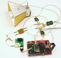
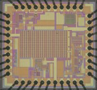
A 1 Mbps 916.5 MHz OOK transceiver for wireless sensor networks has been designed in a 0.18-µm CMOS process. The RX has an envelope detection based architecture with a highly scalable RF front end. The RX power consumption scales from 0.5 mW to 2.6 mW, with an associated sensitivity of -37 dBm to -65 dBm at a BER of 10-3. The TX consumes 3.8 mW to 9.1 mW with output power from -11.4 dBm to -2.2 dBm. The RX achieves a startup time of 2.5 µs, allowing for efficient duty cycling.

Fine Grain Power Domains with Dual-VDD for a Field Programmable Gate Array

Image of chip design
A Field Programmable Gate Array test chip using 0.18µm CMOS contains reconfigurable power domains to optimize active power consumption. Each configurable logic block and routing channel can operate at a choice of 2 voltages to reduce power consumption where longer latencies can be tolerated. On average a 54% reduction in power is achieved.

Sub-threshold SRAM

Image of chip design
A 256kb sub-threshold SRAM operates below 400mV from 0 to 85°C and is implemented in 65nm CMOS technology. For the same 6 sigma static-noise margin, the sub-threshold SRAM at 0.4V achieves 2.25-times lower leakage power and 2.25-times lower active energy than its 6T counterpart at 0.6V. The SRAM uses a 10T bitcell to enable sub-threshold functionality.

500-MS/s 5-bit ADC with Split Capacitor Array

Image of chip design
A 500-MS/s, 5-b analog-to-digital converter (ADC) is implemented in 65nm CMOS technology. The ADC has six time-interleaved successive approximation register (SAR) channels that consume 6 mW from a 1.2 V supply. The ADC is the first implementation of the split capacitor array, replacing the conventional binary-weighted capacitor array of a SAR converter. The new array is faster and lower power without any degradation in linearity.