
A Batteryless Thermoelectric Energy-Harvesting Interface Circuit with 35mV Startup Voltage

Image of chip design
A batteryless thermoelectric energy-harvesting interface circuit to extract electrical energy from human body heat is implemented in a 0.35µm CMOS process. A mechanically assisted startup circuit enables operation of the system from input voltages as low as 35mV. The chip includes a control circuit that performs maximal transfer of the extracted energy to a storage capacitor and regulates the output voltage at 1.8V.

Voltage Scaling in SRAM

Image of chip design
There is a need for large embedded memory that operates over a wide range of supply voltage compatible with the limits of static CMOS logic. This chip demonstrates circuit solutions to voltage scaling in SRAM for both active operation and standby mode in an 8T SRAM fabricated in 45 nm SOI CMOS. The chip exhibits voltage scalable operation from 1.2 V down to 0.57 V with access times from 400 ps to 3.4 ns. Timing variation and the challenge of low voltage operation are addressed with an AC-coupled sense amplifier. An area efficient data path is achieved with a regenerative global bitline scheme. Finally, a data retention voltage sensor has been developed to predict the mismatch-limited minimum standby voltage without corrupting the contents of the memory.

An Efficient Piezoelectric Energy Harvesting Interface Circuit using a Bias-Flip Rectifier and Shared Inductor

Image of chip design
A bias-flip rectifier that can improve the power extraction capability from piezoelectric harvesters over conventional full-bridge rectifiers by 4.2× is implemented in a 0.35µm CMOS process. An efficient control circuit to regulate the output voltage of the rectifier and recharge a storage capacitor is presented. The inductor used within the bias-flip rectifier is shared efficiently with switching DC-DC converters reducing the overall component count.

SoC for Chronic Seizure Detection

Image of chip design
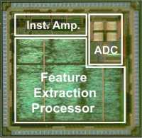
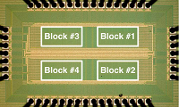
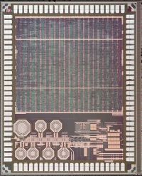
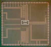
The IC is fabricated in 180nm 5M2P CMOS and operates at 1V. It includes a low-noise instrumentation amplifier for electroencephalograph (EEG) acquisition, an ADC, and a custom digital processor. The instrumentation amplifier uses a chopper-stabilized first stage with a power consumption of 3.5µW and a noise PSD of 130nV/sqrt(Hz). Its input impedance is >700MOhm making it suitable for surface EEG acquisition using Ag/AgCl electrodes. The ADC consumes 250nJ for each 12-bit conversion (10.6 ENOB). The processor includes a decimation filter and a spectral-analysis FIR filter bank to extract spectra-energy features for continuous seizure detection.

A 45nm 0.5V 8T Column-Interleaved SRAM with on-Chip Reference Selection Loop for Sense-Amplifier

Image of chip design
8T bit-cells hold great promise for overcoming device variability in deeply scaled SRAMs and enabling aggressive voltage scaling for ultra-low-power. This work presents an array architecture and circuits with minimal area overhead to allow column-interleaving while eliminating the half-select problem. This enables sense-amplifier sharing and soft-error immunity. A reference selection loop is designed and implemented in the column circuitry. By choosing one of the two reference voltages for each sense-amplifier in a pseudo-differential scheme, selection loop effectively reduces input offset. 8T test array fabricated in 45nm CMOS achieves functionality from 1.1V to below 0.5V. Test chip operates at 450MHz at 1.1V and 5.8MHz at 0.5V while consuming 12.9mW and 46µW respectively.

A Pulsed UWB Receiver SoC for Insect Flight Control

Image of chip design
A highly integrated, 3-to-5 GHz non-coherent pulsed UWB Rx SoC is designed for an insect flight control system. The SoC includes an integrated 4-channel PWM stimulator. The highly duty cycled Rx requires 0.5 to 1.4nJ/bit. Amultistage tuned-inverter based RF front end and differential signal chain allows for robust, low energy operation. The receiver achieves a maximum sensitivity of -76dBm at a data rate of 16Mb/s (10-3 BER).

A 0.16mm2 Completely On-Chip Switched-Capacitor DC-DC Converter Using Digital Capacitance Modulation for LDO Replacement in 45nm CMOS

Image of chip design
A completely on-chip switched-capacitor DC-DC converter that occupies 0.16mm2 is implemented in a 45nm CMOS process. The converter delivers 8mA output current while maintaining load voltages from 0.8 to 1V from a 1.8V input supply. A digital capacitive modulation scheme is employed to maintain the converter efficiency above 60% over a wide range of load current levels.