Computational photography applications significantly extend and enhance the capabilites of existing cameras. The high computational complexity of such multimedia processing applications necessitates fast hardware implementations to allow real-time processing. This work implements a reconfigurable multi-application processor to enable energy-efficient real-time computational photography on portable multimedia devices. The reconfigurable hardware implements Bilateral filtering - a non-linear filtering technique with wide range of computational photography applications, and implements it using a Bilateral Grid structure, which represents an image using a 3D data structure and filters it using a 3D Gaussian kernel. The processor implements High Dynamic Range (HDR) imaging, Low-Light Enhancement, by merging flash and non-flash images such that the natural scene ambience is preserved while achieving high details and low noise, and Glare Reduction. The filtering engine can also be accessed from off-chip and used with other applications.
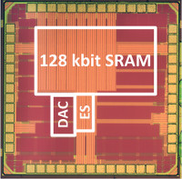
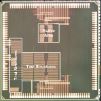
The implementation significantly accelerates bilateral filtering and enables various edge-aware image processing applications in real-time on HD images. The processor, implemented using 40 nm CMOS technology, is operational from 25 MHz at 0.5 V to 98 MHz at 0.9 V. The testchip achieves 13 megapixel/s throughput while consuming 1.4 mJ/megapixel energy at 0.9 V - a significant energy reduction compared to CPU/GPU implementations.