
An Energy-Scalable Accelerator for Blind Image Deblurring

Image of chip design
Camera shake is the leading cause of blur in cell-phone camera images. Removing blur requires deconvolving the blurred image with a kernel which is typically unknown and needs to be estimated from the blurred image. This kernel estimation is computationally intensive and takes several minutes on a CPU which makes it unsuitable for mobile devices. This work presents the first hardware accelerator for kernel estimation for image deblurring applications. Our approach, using a multi-resolution IRLS deconvolution engine with DFT based matrix multiplication, a high-throughput image correlator and a high-speed selective update based gradient projection solver, achieves a 78x reduction in kernel estimation runtime, and a 56x reduction in total deblurring time for a 1920x1080 image enabling quick feedback to the user. Configurability in kernel size and number of iterations gives up to 10x energy scalability, allowing the system to trade-off runtime with image quality. The test chip, fabricated in 40 nm CMOS, consumes 105 mJ for kernel estimation running at 83 MHz and 0.9 V, making it suitable for integration into mobile devices.

A Reconfigurable Conditional Pre-Charge 16kbit SRAM in 28nm FD-SOI

Image of chip design
This work presents a data-dependent SRAM paired with statistical methods to leverage data correlation for the purpose of low power read operations. A 10T bit-cell, a prediction-based conditional pre-charge circuit, and a compact column circuit implemented in a 16kbit 28nm SRAM test chip demonstrate power savings up to 69% for applications spanning signal processing, video coding and computer vision as compared to similar memories with naive prediction.

Nanowatt Circuit Interface to Whole-Cell Bacterial Sensors

Image of chip design
In this work we designed a nanowatt-level readout system for bioluminescence measurements from bacterial cells. The system achieves 600 nJ/conversion from external NPN phototransistors with an effective photon noise flux of 5.3 × 10⁵ ph/mm². The system can successfully detect bioluminescence produced by engineered heavy-metal sensing bacteria using 4.0 × 10⁶ cells in 15 µL of sample.

A Low-Noise Instrumentation Amplifier for Sensors using a Noise-Efficient 0.2V-Supply Input Stage

Image of chip design
In low-bandwidth, low-noise applications of wireless sensor nodes, the sensor front-end amplifier presents a power consumption bottleneck since its current draw is noise-limited and cannot be scaled with the low data rate, as is possible with the DSP and RF blocks. Prior work to improve the energy-efficiency of low-noise instrumentation amplifiers (LNIAs) for sensors includes chopper IAs, inverter-based LNAs, current-reuse through amplifier stacking, and low supply voltage amplifier design reaching 0.45V. This work presents an analog front-end (AFE) that achieves an Power Efficiency Figure (PEF) of 1.6 by using a chopper LNIA with a 0.2V-supply inverter-based input stage followed by a 0.8V-supply folded-cascode common-source (FCCS) stage. The high input-stage current needed to reduce the input-referred noise is drawn from the 0.2V supply, significantly reducing power consumption. The 0.8V stage provides high gain and signal swing, improving linearity.

A 0.6V 8mW 3D Vision Processor for a Navigation Device for the Visually Impaired

Image of chip design
3D imaging devices, such as stereo and time-of-flight (ToF) cameras, measure distances to the observed points and generate a depth image where each pixel represents a distance to the corresponding location. The depth image can be converted into a 3D point cloud using simple linear operations. This spatial information provides detailed understanding of the environment and is currently employed in a wide range of applications such as human motion capture. However, its distinct characteristics from conventional color images necessitate different approaches to efficiently extract useful information. This chip is a low-power vision processor for processing such 3D image data. The processor achieves high energy-efficiency through a parallelized reconfigurable architecture and hardware-oriented algorithmic optimizations. The processor will be used as a part of a navigation device for the visually impaired. This handheld or body-worn device is designed to detect safe areas and obstacles and provide feedback to a user. We employ a ToF camera as the main sensor in this system since it has a small form factor and requires relatively low computational complexity.

A Keccak-based Wireless Authentication Tag with Per-Query Key Update and Power-Glitch Attack Countermeasures

Image of chip design
This chip is a wireless authentication tag for supply chain integrity applications. Since the tags are intended to be used for anti-counterfeiting countermeasures against physical attacks are crucial. The tag implements FeCap based NV-DFFs along with an on-chip energy backup solution. This when combined with a custom key update protocol provides resilience against side-channel and power glitch attacks. The tag also implements a new regulating voltage multiplier topology and pulse position modulation for efficient power and data-transfer over a 433MHz near field inductive link.

A 0.36V Energy-Efficient 128Kb 6T SRAM with Output Data Prediction in 28nm FDSOI

Image of chip design
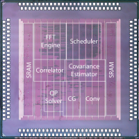
The aggressive scaling of SRAM bit-cell size with every technology node makes it extremely challenging to reduce the Vdd,min of SRAMs, due to the increasing effect of device variations. However, Vdd scaling is crucial in reducing the energy consumption of SRAMs, which is a significant portion of the overall energy consumption in modern micro-processors. Energy savings in SRAM are particularly important for battery-operated applications, which run from a very constrained power-budget. This work presents a low-voltage, energy-efficient SRAM designed in a 28nm fully depleted SOI (FDSOI) technology. The SRAM achieves a minimum Vdd of 0.36V, while still having the area advantage by using 6T bit-cells. Dynamic forward body-biasing is used to improve the Vdd,min. Improved array layout helps in reducing the switching energy. An average energy/bit-access of 52.5fJ has been achieved at 0.45V. Furthermore, by implementing data prediction in the read-path, up to 36% dynamic energy savings are obtained.