
A Switched Capacitor DC-DC Converter for ultra-low-power applications

Image of chip design
A switched capacitor DC-DC converter that could deliver scalable output voltages was designed in National Semiconductor's 0.18µm CMOS process. The converter was able to deliver load voltages from 0.3V - 1.1V and was powered by a 1.2V battery. It employs on-chip charge transfer capacitors and reduces the loss due to bottom-plate parasitics by employing a method known as divide-by-3 switching.

CMOS interface to CNT sensor arrays

Image of chip design
The interface chip attains a large dynamic range using an ADC and DAC of lower dynamic range and an automatic gain control. The sensor interface chip is designed in a 0.18µm CMOS process and consumes, at maximum, 32 µW at 1.83 kS/s conversion rate. The designed interface achieves 1.34% measurement accuracy over 10 kOhm - 9 MOhm dynamic range. The power consumption of the chip can be linearly scaled using duty-cycling.

A 6-bit, 0.2V to 0.9V Highly Digital Flash ADC with Comparator Redundancy

Image of chip design
A 6-bit highly digital flash ADC is implemented in a 0.18µm CMOS process. The ADC operates in the subthreshold regime down to 200mV and employs comparator redundancy to improve linearity. Common-mode rejection is implemented digitally via an IIR filter. The ADC's minimum FOM is at a supply of 0.4V, where it achieves a FOM of 125fJ/conversion-step and a ENOB of 5.05 at 400kSPS.

A 256kb 65nm 8T Sub-Threshold SRAM Employing Sense-Amplifier Redundancy

Image of chip design
An 8T SRAM achieves full read and write functionality at 350mV. The read-buffered bit-cell eliminates the read static noise margin limitation; peripheral control of the read-buffer eliminates sub-Vt bit-line leakage from unaccessed cells; peripheral control of the bit-cell supply voltage ensures write-abilty in the presence of variation; and the technique of sense-amplifier redundancy improves the area-offset tradeoff in the sensing network by over a factor of 5.

A 3.1-5GHz All-Digital UWB Transmitter

Image of chip design
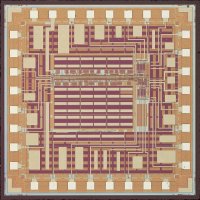
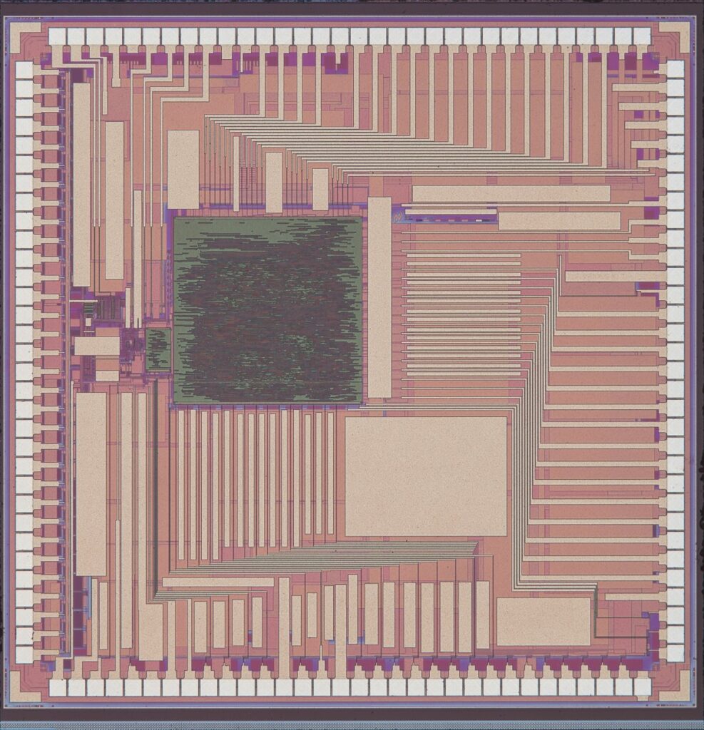
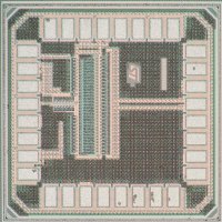
This chip demonstrates an all-digital technique for generating UWB pulses with a programmable width and a center frequency tunable to 3 channels in the 3.1-5GHz band without the use of an RF oscillator. A delay-based spectral scrambling technique is proposed and implemented in this chip that exploits the delay-line based digital architecture to scramble the output spectrum. The main advantage of this scrambling technique is a drastic reduction of the hardware required to implement it, relative to the more commonly used BPSK scrambling. The transmitter uses only digital blocks, including the final stage driving the 50Ohm UWB antenna, which is a digital pad driver. The circuit consumes a total of 43pJ/bit at a data rate of 16.7Mb/s, including all core, control, and I/O power.

A 2.5nJ/b 0.65V 3-to-5GHz Subbanded UWB Receiver in 90nm CMOS

Image of chip design
The IC is a non-coherent 0-to-16Mb/s UWB receiver using 3-to-5GHz subbanded PPM signaling implemented in a 90nm CMOS process. The RF and mixed-signal baseband circuits operate at 0.65V. Using duty-cycling, adjustable BPFs, and an energy-aware baseband, the receiver achieves 2.5nJ/b and 10-3 BER with -99dBm sensitivity at 100kb/s.

A 400-mV UWB Baseband Processor

Image of chip design
The baseband processor performs acquisition and demodulation of an UWB packet with a throughput of 500-MS/s for a data-rate of 100-Mb/s. It operates at an ultra-low supply voltage of 400-mV to achieve 20 pJ/bit, and utilizes a highly parallelized architecture to meet throughput constraints. It was fabricated in a standard-VT 90-nm CMOS process.

Minimum Energy Tracking Loop with Embedded DC-DC Converter

Image of chip design
An energy minimization loop, with on-chip energy sensor circuitry, that can dynamically track the minimum energy operating voltage of a digital circuit with changing workload and operating conditions occupies 0.05mm2 in 65nm CMOS. The DC-DC converter that enables this minimum energy operation can deliver load voltages as low as 250mV and achieved an efficiency >80% while delivering load powers of the order of 1µW and higher from a 1.2V supply.